Huangpu district teams up with chip giant

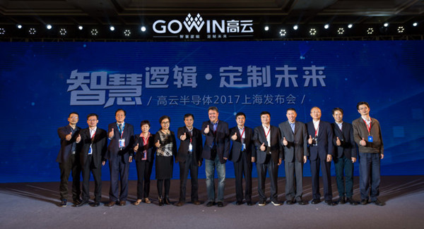
Huangpu district in the southern Chinese city of Guangzhou, signed an investment contract with chip giant Guangdong Gowin Semiconductor Corp (Gowin), in Shanghai on Oct 26.
Headquartered at the district's Guangzhou Science City, Gowin plans to make good use of the high-tech industry and market resources in Huangpu district. The company's high-end chip FPGA (Field–Programmable Gate Array) technology and industrial advantages will also be used to boost the development and application of emerging technologies in Huangpu.
FPGA is an integrated circuit designed to be configured by a customer or a designer after manufacturing. FPGAs contain an array of programmable logic blocks, and a hierarchy of reconfigurable interconnects that allow the blocks to be "wired together", like many logic gates that can be inter-wired in different configurations.
Founded in 2014, Gowin adheres to the principle of independent development and research and has founded the only team that has mastered FPGA technology in the country, releasing more than 50 encapsulated types of FPGA chips. Gowin has intellectual property rights over all its products, breaking up international monopolies and making China the second country to develop and produce FPGA chips.
Gowin has a complete industrial layout at its headquarters in Guangzhou, and has research and development centers in Shanghai, Jinan in Shandong province and Silicon Valley in the US, as well as sales centers in Shenzhen and Hong Kong.
Based on the extant integrated circuit industry in Huangpu, Gowin is expected to boost the development of consumer electronics, industrial control and equipment manufacturing in the area by forming a complete chain integrating FPGA design, production, packing and testing, application development and solutions.

Huangpu district signs an investment contract with chip giant Gowin in Shanghai on Oct 26. [Photo provided to chinadaily.com.cn]


